Sidebar
Filter
PCB Inspection System

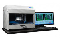
Novascope Semi-Automated Optical Inspection System
The NovaScope is a semi-automated optical inspection and image archiving system for PCBs (printed circuit boards). It significantly increases the speed and accuracy of manual visual inspections, and is a fraction of the price of a fully automated AOI. Programming can be done in a matter of minutes using the integrated Gerber, XY Placement List, and Bill of Materials import features. There is also a utility for simple matrix type scanning & inspecting of the board.
Your Economic Solution for Control of your PCB Inspection Process: This machine is a perfect fit for low volume PCB assembly, and prototype applications, especially those with unique board features.
- Less operator fatigue
- Less board handling
- 100% accuracy
- 100% traceability
- 100% operator control
- Benefits outweigh cost
The NovaScope is a powerful PCB inspection station for:
- High Reliability applications (MIL-Spec, Medical, Automotive)
- Hi-Mix Low-Volume operations
- First Article Inspection
- Solder Joints and Tall Thru-hole Parts
- Photo Documentation for traceability
- Conformal Coating Inspections
- Assembly Line Auditing
- Cleanliness/FOD/Tin Whisker detection
How it works:
The optical inspection system automatically moves a digital microscope to the PCB inspection points, sets the lighting, camera height and angle, zooms to the region of interest, and displays a live image of the inspection area. The images are automatically captured and can be stored as part of a post inspection report.
The inspection can be done by component, by board region, or by a combination of both. Inspections can be performed for many reasons: verify part presence, rotation, polarity, registration, text, solder, solder paste, bent leads, bent pins, jumpers, cut traces, or any other top down or side visual feature on the PCB.
NovaScope Semi-Auto Optical Inspection
With complete control of your inspection process, you won't miss a spot. The camera can be programmed to move sequentially, detecting Absence or Presence of hardware, screws, wire routings, foreign objects, damage and debris.
Or, if you just want to pick out problem areas for 'speed' of efficiency - that's OK too. Programs can be run to search designated areas of the board, vs the selection of individual components.
